

Expert Semiconductor Engineering Services
Discover our specialized technical consulting and equipment recovery solutions designed for maximum uptime and reliability.
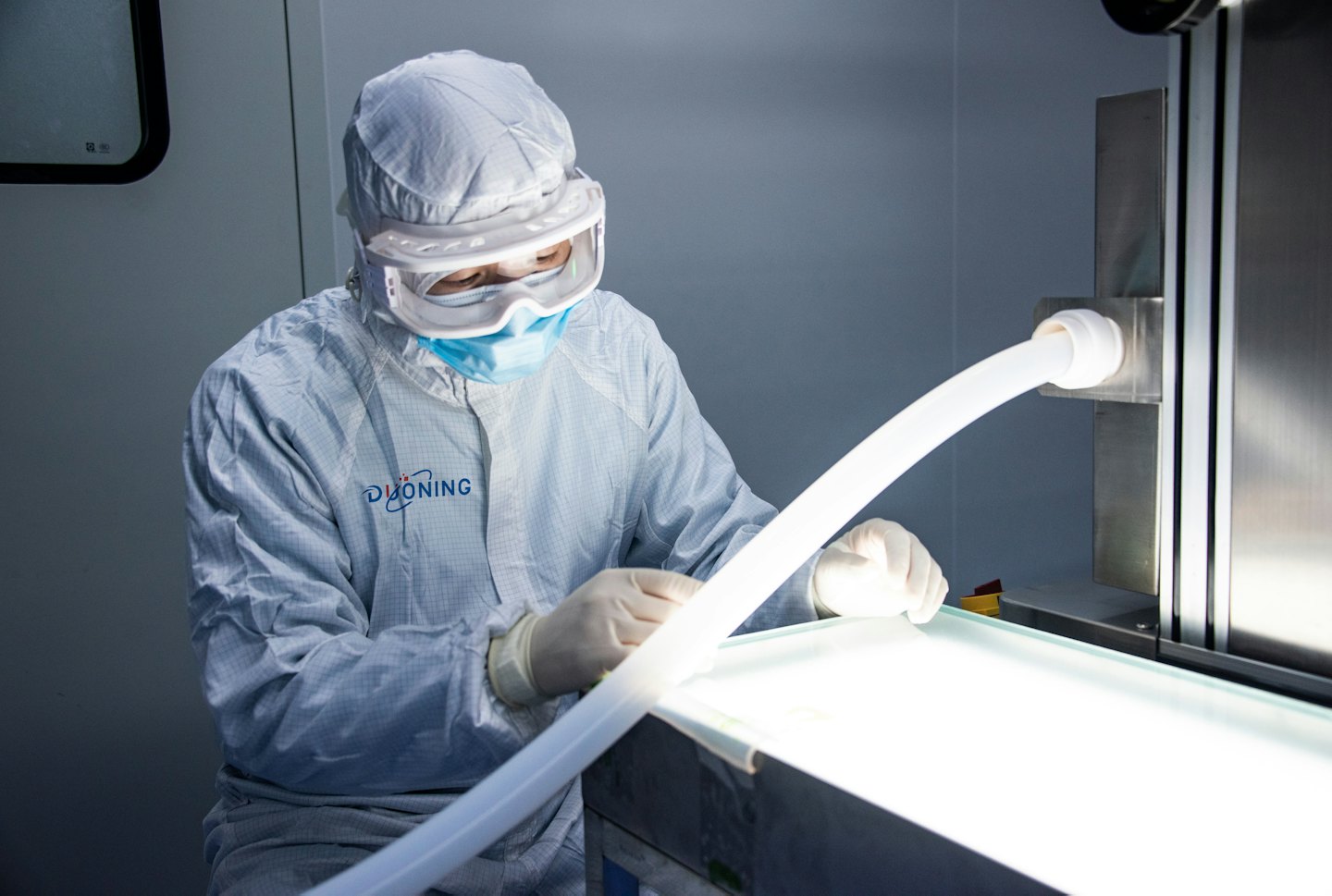
Deposition Equipment
Advanced troubleshooting and optimization for PVD, CVD, PECVD, SACVD, and tungsten deposition systems.
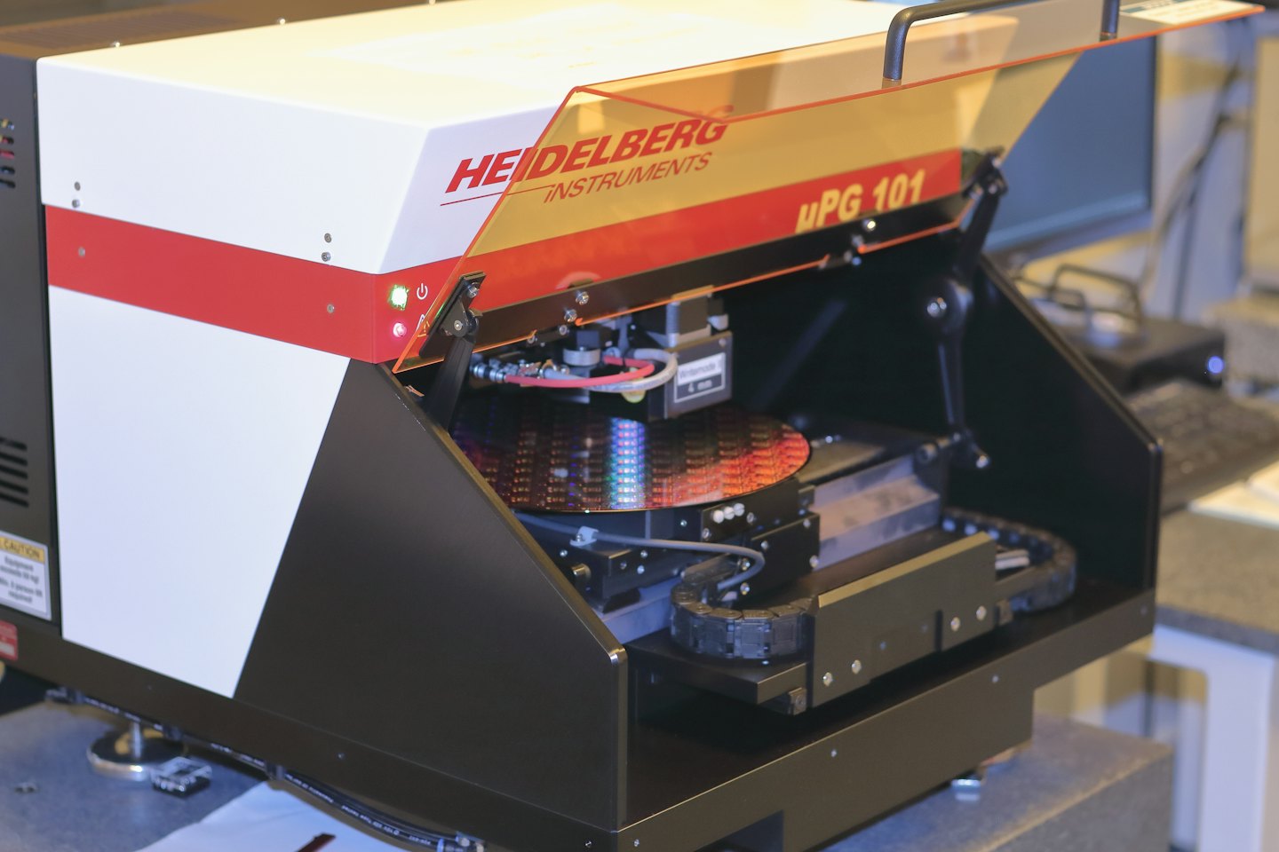
Vacuum Systems
Comprehensive diagnosis and repair for complex vacuum architectures and associated delivery lines.

Equipment Recovery
Specialized intervention to restore tools from extended downtime and resolve stubborn technical issues.
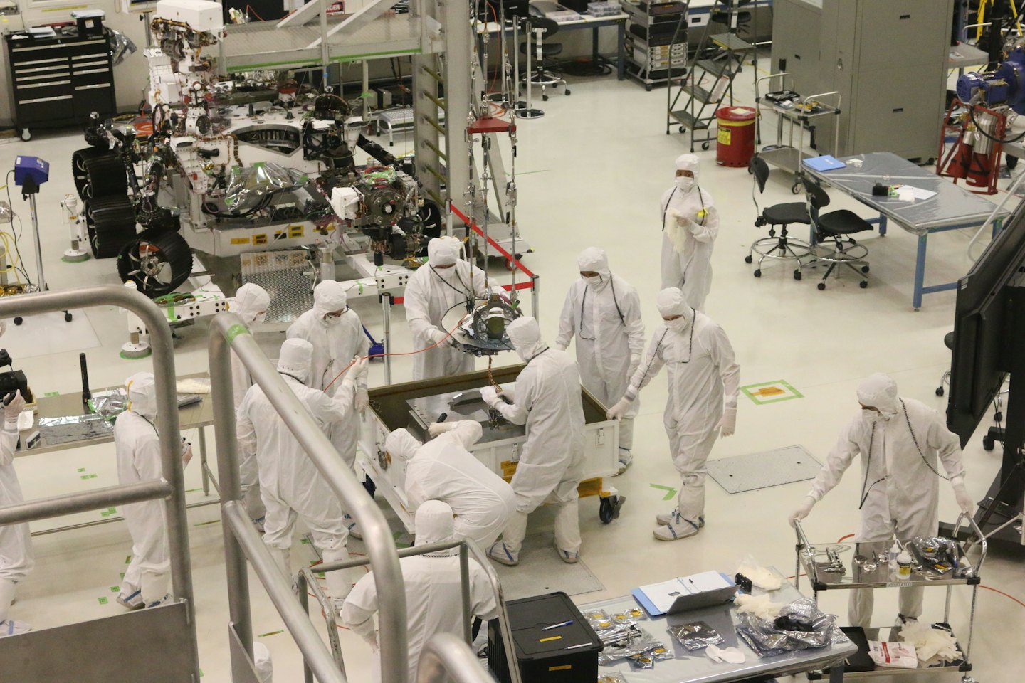
Plasma & Robotics
Precision engineering support for RF plasma systems, thermal controls, and automated wafer robotics.
Our Process
Our systematic approach ensures complex semiconductor manufacturing equipment failures are diagnosed accurately and downtime is minimized.

Diagnostic Assessment
We thoroughly evaluate deposition equipment and vacuum systems to uncover the root cause when conventional troubleshooting falls short.

Equipment Recovery
Our experts execute targeted repairs and optimization for PVD, CVD, and plasma systems to restore your fabrication line efficiently.

Technical Resolution
We resolve recurring technical problems to ensure long-term reliability and peak performance for your facility.
Expert Engineering Solutions for Semiconductor Manufacturing
Leveraging thirty years of hands-on semiconductor experience, we diagnose complex equipment failures, recover systems from extended downtime, and resolve recurring technical problems when conventional troubleshooting falls short.
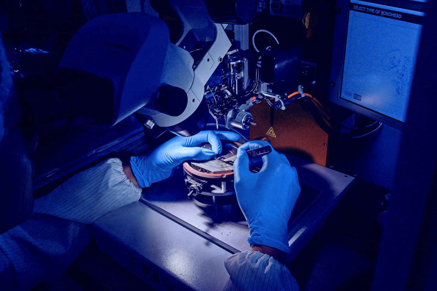
PVD and CVD Expertise
Deep technical mastery in physical and chemical vapor deposition, PECVD, SACVD, and advanced tungsten deposition processes for fabrication facilities.
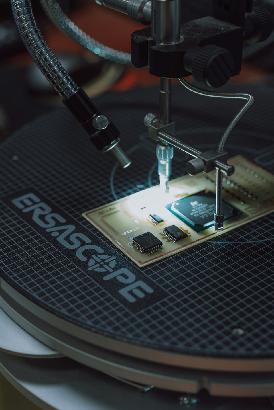
Vacuum & Gas Delivery
Comprehensive diagnosis and optimization of complex vacuum systems, gas and liquid delivery networks, and thermal control infrastructure.
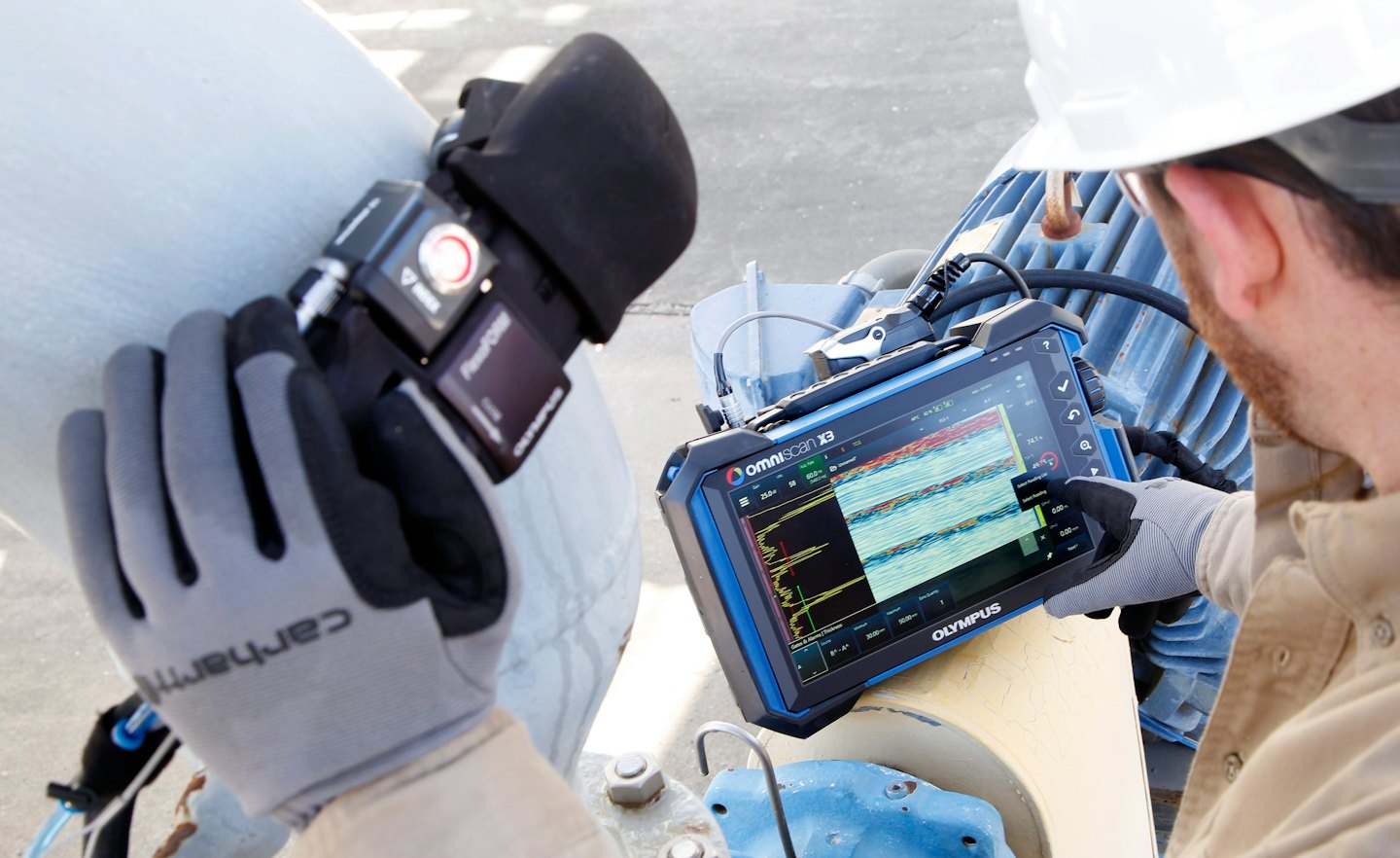
RF Plasma & Robotics
Specialized troubleshooting for RF plasma systems and precision semiconductor robotics to eliminate recurring downtime and restore peak output.